Why Heterogeneous Parallel Computing
Heterogeneous Parallel Computing
Two trajectories -- multiple cores and many threads
Since 2003, industry has settled on two main trajectories for designing microprocessors.
- multicore trajectory seeks to maintain the execution speed of sequential programs while moving into multiple cores. e.g. ARM Ampere multicore server processor with 128 processor cores.
- many-thread trajectory focus more on the execution throughput of parallel applications. The NVIDIA Tesla A100 GPU has has tens of thousands of threads, executing in a large number of simple, in-order pipelines.
Peak performance gap
As of 2021, the peak floating-point throughput of the NVIDIA Tesla A100 GPU is 9.7 TFLOPS for 64-bit double-precision, 156 TFLOPS for 32-bit single-precision, and 312 TFLOPS for 16-bit half . In comparison, the peak floating-point throughput of the recent Intel 24-core processor is 0.33 TFLOPS for double-precision and 0.66 TFLOPS for single-precision.
| 64-bit double-precision | 32-bit single-precision | 16-bit half-precision | |
|---|---|---|---|
| NVIDIA A100 GPU | 9.7 TFLOPS | 156 TFLOPS | 312 TFLOPS |
| Intel 24-core processor | 0.33 TFLOPS | 0.66 TFLOPS | - |
Such a large Gap in peak performance has already motivated many applications developers to move the computationally intensive parts of their software to GPU for execution.
Different design philosophies between CPU & GPU
One might ask why there is such a large peak performance gap between many-thread GPUs and multicore CPUs. The answer lies in the differences in the fundamental design philosophies between the two types of processors, as illustrated below.
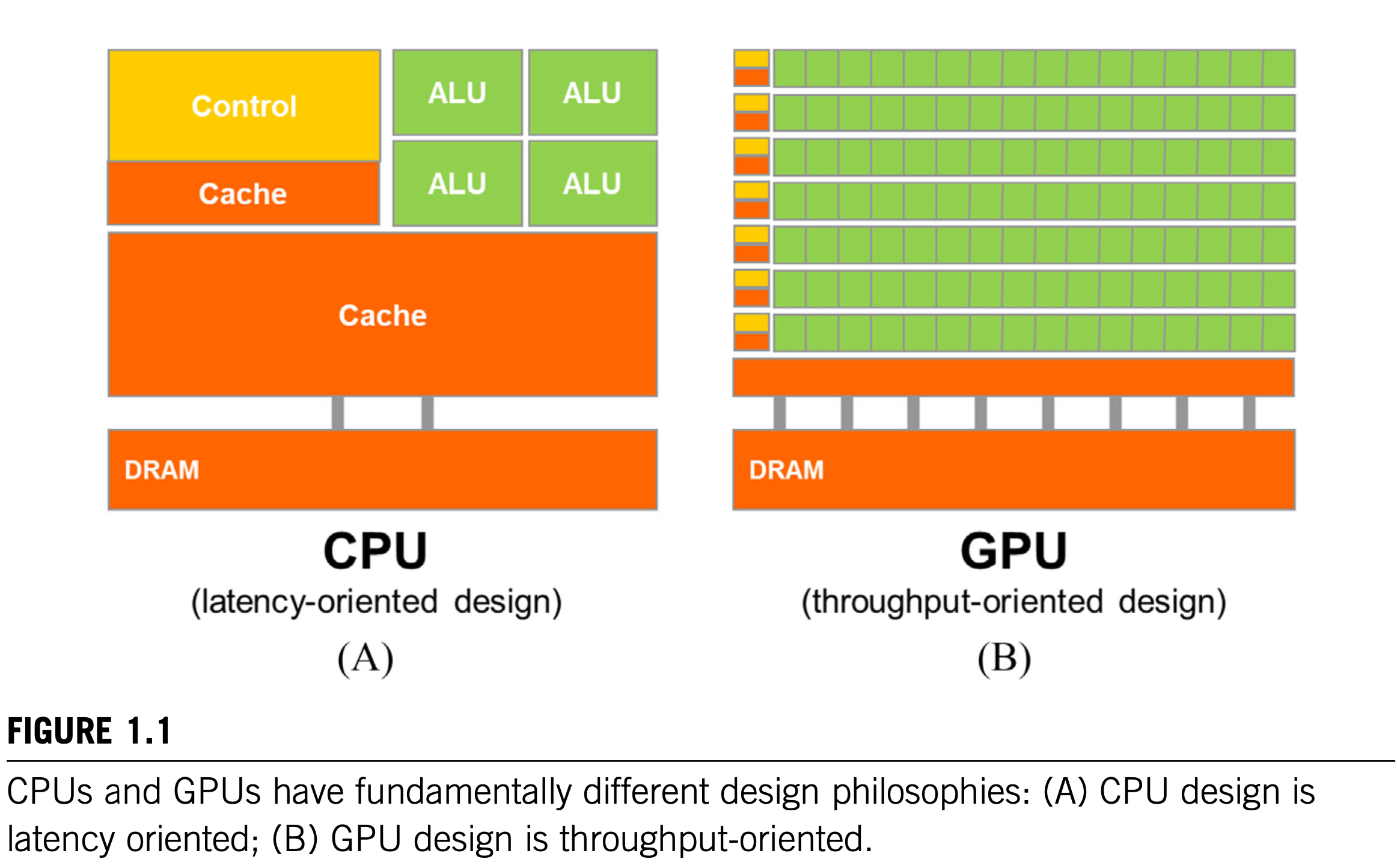
CPU: latency-oriented design
The design of CPU is optimized for sequential code performance:
- The arithmetic units and operand data delivery logic are designed to minimize the effective latency of arithmetic operations at the cost of increased use of chip area and power per unit.
- Large last-level on-chip caches are designed to capture frequently accessed data and convert some of the long-latency memory access into short-latency cache accesses.
- Sophisticated branch prediction logic and execution control logic are used to mitigate the latency of conditional branch instructions. This design approach is commonly referred to as latency-oriented design. By reducing the latency of operations, the CPU hardware reduces the execution latency of each individual thread. However, the low-latency arithmetic units, sophisticated operand delivery logic, large cache memory, and control logic consume chip area and power that could otherwise be used to provide more arithmetic execution units and memory access channels. 🤯🤯🤯!
GPU: throughput-oriented design
The design philosophy of GPUs, on the other hand, has been shaped by the fast-growing video game industry, which experts tremendous economic pressure for the ability to perform a massive number of floating-point calculations and memory access per frame in advanced games. This demand motivates GPU vendors to look for ways to maximize the chip area and power budget dedicated to floating-point calculations and memory access throughput.
- A GPU must be capable of moving extremely large amount of data into and out of graphics frame buffers in its DRAM (dynamic random-access memory). The relaxed memory model (the way in which various system software, applications, and I/O devices expect their memory access to work) that is commonly accepted by game applications also makes it easier for the GPUs to support massive parallelism in accessing memory. In contrast, general-purpose processors must satisfy requirements from legacy operating systems, applications, and I/O devices that present more challenges to supporting parallel memory accesses and thus make it more difficult to increase the throughput of memory accesses, commonly referred to as memory bandwidth. As a result, graphics chips have been operating at approximately 10 times the memory bandwidth of contemporaneously available CPU chips, and we expect that the GPUs will continue to be at an advantage in terms of memory bandwidth for some time.
- An import observation is that reducing latency is much more expensive than increasing throughput in terms of power and chip area. Therefore the prevailing solution in GPUs is to optimize for the execution throughput of massive numbers of threads rather than reducing the latency of individual threads. This design approach saves chip area and power by allowing pipelined memory channels and arithmetic operations to have long latency. The reduction in area and power of the memory access hardware and arithmetic units allows the GPU designers to have more of them on a chip and thus increase the total execution throughput. There are smaller number of larger arithmetic units and a smaller number of memory channels in the CPU design, in contrast to the larger number of smaller arithmetic units and a larger number of memory channels in the GPU design. The application software for these GPUs is expected to be written with a large number of parallel threads. The hardware takes advantage of the large number of threads to find work to do when some of them are waiting for long-latency memory access or arithmetic operations. Small cache memories in GPU are provided to help control the bandwidth requirements of these applications so that multiple threads that access the same memory data do not all need to go to the DRAM. This design style is commonly referred to as throughput-oriented design, as it strives to maximize the total execution throughput of a large number of threads while allowing individual threads to take a potentially much longer time to execute.
CUDA
It should be clear that GPUs are designed as parallel, throughput-oriented computing engines, and they will not perform well on some tasks on which CPUs are designed to perform well. For programs that have one or very few threads, CPUs with lower operation latencies can achieve much higher performance than CPUs. When a program has a large number of threads, GPUs with higher execution throughput can achieve much higher performance than CPUs. Therefore one should expect that many applications use both CPUs and GPUs. This is why the Compute Unified Device Architecture (CUDA) programming model, introduced by NVIDIA in 2007, is designed to support joint CPU-GPU execution of an application.